
What's TPU? Google Surges Ahead in AI Chip Race with TPU Patent Boom
Google is strengthening its position in the AI hardware race as patent filings for its Tensor Processing Unit (TPU) technology soar, outpacing major rivals like Amazon, Apple, and Microsoft.
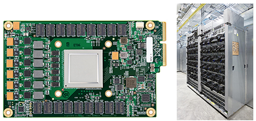 |
Google’s first Tensor Processing Unit (TPU) on a printed circuit board (left); TPUs deployed in a Google datacenter (right). Source: Google Cloud Blog |
Analysts at TrendForce predict Google’s TPU shipments will lead the cloud industry, growing more than 40% annually by 2026. The move signals a broader industry shift as hyperscalers develop custom chips tailored for massive AI workloads.
Expanding the Supply Chain
To meet demand, Google’s chip partners Broadcom and MediaTek are ramping up wafer production through TSMC’s advanced 3nm process. The eighth-generation TPUs are expected to enter mass production in mid-2026, with projected output nearing 5 million units in 2027.
Meta is reportedly negotiating a multi-billion-dollar deal with Google to adopt TPUs in its data centers as early as 2027. Meanwhile, AI firm Anthropic has already signed a major agreement to access up to 1 million TPUs, marking Google’s growing foothold in the AI hardware market.
GPU vs. TPU: What’s the Difference?
-
GPU (Graphics Processing Unit): Originally built for rendering graphics, GPUs excel at handling many small, parallel tasks — ideal for training large AI models but often power-hungry and costly.
-
TPU (Tensor Processing Unit): Designed by Google specifically for AI and machine learning, TPUs handle tensor computations more efficiently. They deliver faster performance and lower energy use for operations like deep neural network processing.
In short, GPUs are general-purpose accelerators, while TPUs are specialized engines built for AI — giving Google a custom advantage in speeding up model development and cutting infrastructure costs.


